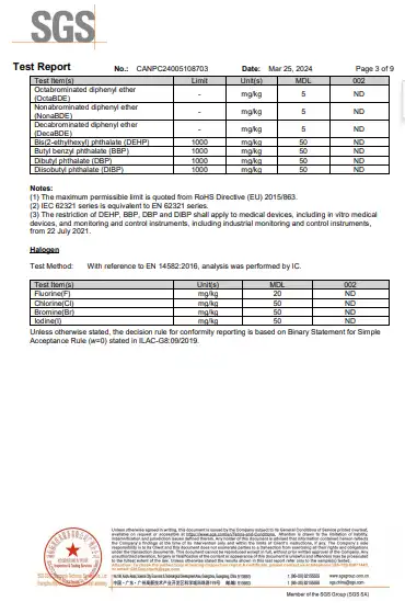
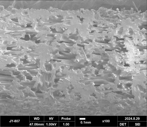
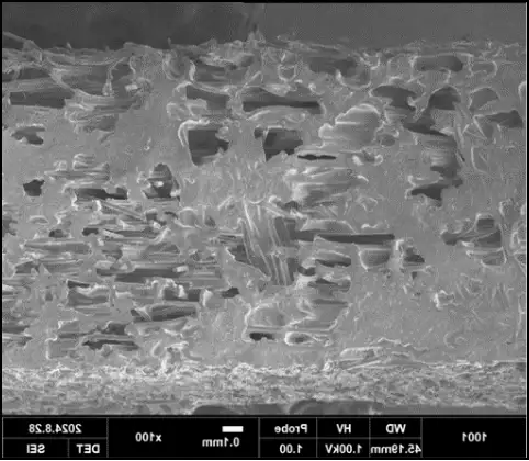
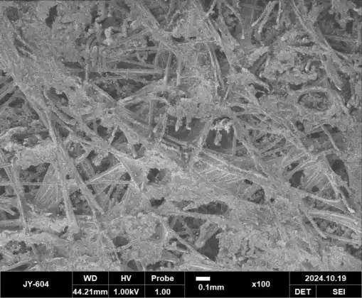
Intech Technology Group Ltd.

Precision
CMP Consumables
for Semiconductor

YX Semiconductor Materials provides high-performance polishing pads and waxless templates for wafer CMP processes. Our solutions support silicon, SiC, GaAs, sapphire, and other advanced semiconductor materials.

2021
Est. Year
9,500
Total Facilities
2
Production Bases
About Us

High-Tech CMP
Consumables Leader

YX Semiconductor Materials Co., Ltd. (est. June 2021) is based in Humen, Dongguan, with advanced manufacturing and testing equipment. As a high-tech enterprise focusing on semiconductor CMP consumables — R&D, production, and sales — we optimize polishing processes for clients worldwide.

Jiangsu R&D Hub

Dongguan Base

Humen, Dongguan · Est. 2021

4,500 sqm facility featuring comprehensive cleanroom manufacturing (ISO Class 8 / Class 100,000) and state-of-the-art testing systems.

4,500
sqm
ISO 8
Cleanroom
5S
Management
Jiangsu R&D Hub

Jiangsu Base

Jiangsu Province · Est. 2023

5,000 sqm R&D and production hub pioneering domestic substitution of high-end semiconductor consumables with international technical cooperation.

5,000
sqm
R&D
Focus
Intl.
Cooperation
CMP POLISHING PAD

Customized solutions for CMP machine and CMP application

Stock Polishing Pad

YXPDBMC Series

The YXPDBMC Series of polishing pads withnonwoven bases are primarily used for stock polishing.These pads stand out for their high removal rate,highlevel of flatness,and low defectivity.

YXPDBMC49 显微结构图

SIC Polishing Pad

YXPDBMC49

Thickness 1.32 mm
Density 0.52 g/cm³
Compressibility 3.5%
Compressed elasticity 52.6 %
Hardness (Asker-C) 87.2
YXPDBMC42 显微结构图

SILICON Stock Polishing

YXPDBMC42

Thickness 1.30 mm
Density 0.46 g/cm³
Compressibility 4.5%
Compressed elasticity 69.5 %
Hardness (Asker-C) 82.7
YXPDBMC47 显微结构图

SIC STOCK POLISHING

YXPDBMC47

Thickness 1.31 mm
Density 0.57 g/cm³
Compressibility 2.5%
Compressed elasticity 50.8 %
Hardness (Asker-C) 92.5
Waxless template solution

A Superior Waxless Alternative to Legacy Mounting Methods

Each unit is constructed by bonding a precison-machined framework to a specailized porous backing layer, ensuring secure wafer retention.

By leveraging proprietary manufacturing techniques that ensure exceptional material uniformity, our solution delivers process stability and performance consistency that exceed current industry benchmarks.

Waxless Polishing Template

Waxless template sample 1
Waxless template sample 2
Waxless template sample 3
Waxless template sample 4
Single-Sided Processing
Surface Application
Buffed

Final Polish

Acts as a cushion to remove micro-scratches and improve surface haze.

Non-Buffed

Stock Removal

Acts as a rigid backstop to correct Total Thickness Variation (TTV) and achieve superior flatness.

Silicone

Specialized for Compound Semiconductors (e.g., GaAs, InP). Prevents corrosive slurry from wicking to the wafer backside (Anti-wicking).

These single sided waxless templates can be customized to accommodate any type of material and polishing equipment.

Waxless

Chemically Resistant Waxless Template

The Chemically Resistant Template (CXT) series is engineered specifically to withstand degradation in the harshest polishing environments.

These templates are the ideal solution for processes utilizing aggressive oxidants or operating at extreme pH levels (high acid/alkaline), where standard templates often fail.

CXT Designed for Challenging Process:
low pH slurries/High pressure/High temperature.

Composition Report of Template Material

Composition Report 1 Composition Report 2 Composition Report 3 Composition Report 4

Enterprise Certificate

Enterprise Certificate 1 Enterprise Certificate 2 Enterprise Certificate 3
Contact Us

Let's Work Together

Contact Team

Reach our sales contacts directly for product and application support.

Send an Inquiry

Describe your CMP application and we'll find the optimal solution.